Intel Foundry Wins AMD, NVIDIA and OpenAI Orders as EMIB Yield Hits 98%
Intel Foundry is gaining momentum across both advanced process technology and advanced packaging, strengthening its position as a potential alternative to TSMC. The company has reportedly secured design orders involving its 18A and 14A process nodes from major technology companies, including AMD, NVIDIA, OpenAI, Microsoft, Apple, Meta, Micron, and Marvell.
At the same time, Intel’s 18A process yield has reportedly improved to 85%, while its EMIB-T advanced packaging yield has reached 98%. Together, these improvements address two of the semiconductor industry’s most important manufacturing constraints: leading-edge wafer yields and advanced packaging capacity.
With AI accelerator demand continuing to pressure both advanced-node and packaging capacity, Intel’s progress could give chip designers another option for heterogeneous computing platforms and large-scale AI silicon production.
🏭 Intel Foundry Expands Its Advanced-Node Customer Base #
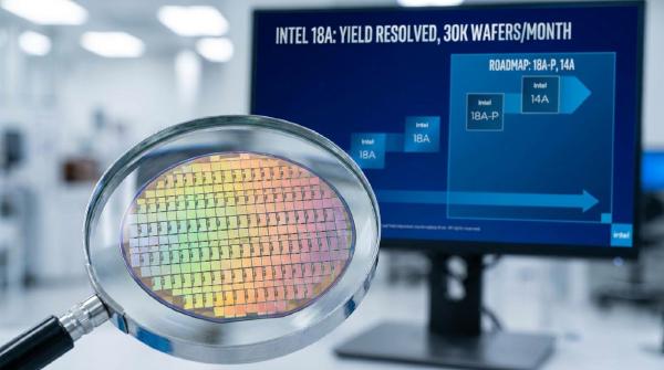
Intel’s 18A process has entered its mass-production ramp, while the more advanced 18A-P variant has moved into risk production. Meanwhile, Intel’s 14A process is expected to enter risk production in 2028, followed by volume manufacturing in 2029.
This process roadmap gives Intel Foundry multiple technology platforms at different stages of maturity. Customers can therefore align their designs with Intel’s near-term manufacturing capabilities while also planning longer-term products around future process generations.
Reports indicate that Intel has secured design orders involving 18A and 14A from several major technology companies, including AMD, NVIDIA, Marvell, Microsoft, Micron, OpenAI, Apple, and Meta.
Design wins provide an important validation signal #
Leading semiconductor and technology companies impose demanding requirements on advanced process technologies, particularly in areas such as performance, power efficiency, transistor density, manufacturing consistency, and long-term supply reliability.
Securing design commitments from these customers therefore represents more than incremental foundry revenue. It provides an important market signal that Intel’s advanced process technologies are becoming sufficiently competitive for high-value commercial designs.
Intel also stands to benefit from the industry’s increasing need for additional advanced-node capacity. TSMC remains the dominant supplier, but sustained AI-related demand has tightened capacity across leading-edge manufacturing and advanced packaging.
A credible second-source option could therefore become strategically valuable for customers seeking additional capacity, supply-chain diversification, or greater negotiating leverage.
Intel 18A yield moves into a commercially viable range #
Intel’s 18A yield has reportedly increased from approximately 65% in the previous quarter to 85%.
For leading-edge semiconductor manufacturing, yield is one of the most important determinants of wafer economics. Higher yield means fewer defective dies per wafer, improving effective manufacturing costs and increasing the number of usable chips available from each production run.
An 85% yield would place 18A within a substantially stronger position for high-volume manufacturing. It remains below the reported approximately 90% yield of TSMC’s N2 process but is significantly above the reported 50–60% range associated with Samsung’s SF2 process.
If Intel can continue improving 18A yield while ramping production, the company could narrow the manufacturing gap with TSMC and gain greater flexibility in pricing and capacity allocation.
📦 EMIB-T Reaches a 98% Yield Milestone #
Intel’s progress is not limited to wafer fabrication. Its EMIB advanced packaging technology is also approaching the yield levels required for large-scale AI chip production.
Intel offers multiple EMIB variants, including EMIB-T and the power-efficiency-focused EMIB-M. These technologies target applications that increasingly depend on integrating multiple compute dies, accelerators, and High Bandwidth Memory within a single package.
EMIB-T targets the advanced packaging bottleneck #
Advanced packaging has become a major constraint on AI semiconductor production. Even when sufficient leading-edge wafer capacity is available, shortages in technologies such as TSMC’s CoWoS can limit the number of complete AI accelerators that can be delivered.
EMIB provides Intel with an opportunity to compete in this segment by integrating multiple dies through a 2.5D packaging architecture.
Reports indicate that EMIB-T’s yield has increased from approximately 90% three months earlier to 98%. Reaching the 98–99% range represents a significant manufacturing milestone because advanced packaging processes must maintain high assembly precision while integrating increasingly complex dies and interconnect structures.
Higher packaging yield reduces the number of failed packages, lowering effective manufacturing costs and improving delivery predictability.
EMIB offers a mature heterogeneous-integration approach #
EMIB has been in mass production since 2017, giving Intel years of experience with its manufacturing and assembly ecosystem.
The technology enables high-density connections between multiple dies, including logic components and HBM, without requiring a conventional large silicon interposer for the entire package.
This approach can simplify certain aspects of heterogeneous integration while providing the flexibility required for increasingly modular chip architectures. As chip designers move toward chiplets, EMIB’s ability to combine different dies within a single package becomes increasingly relevant.
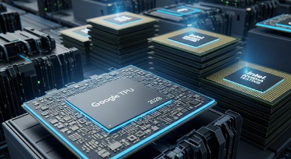
Reported EMIB-based customer programs include NVIDIA’s Feynman GPU, Google’s TPU HumuFish, and Amazon Web Services’ Trainium 3.
The involvement of major AI-computing customers provides additional validation for Intel’s packaging technology and could encourage other chip designers to evaluate EMIB as an alternative advanced-packaging platform.
⚡ Capacity Expansion Targets the AI Computing Boom #
Intel’s process improvements are being accompanied by capacity expansion across multiple manufacturing nodes.
As the 18A production ramp accelerates, Intel is expected to introduce additional products based on the process, including Panther Lake and Wildcat Lake families. Increasing 18A capacity should allow Intel to expand shipments of next-generation client and enterprise products as manufacturing output scales.
Data-center capacity becomes increasingly strategic #
Intel is also expanding capacity for Intel 4 and Intel 3 to support data-center products.
The growth of Agentic AI is expected to increase demand for data-center computing resources, creating additional opportunities for CPU and accelerator suppliers. Some industry estimates project CPU-related demand growth of approximately 25–30% this year, followed by another potential 50% increase next year.
While GPUs and dedicated AI accelerators receive much of the attention surrounding AI infrastructure, CPUs remain essential for orchestration, storage, networking, virtualization, and general-purpose workloads within AI data centers.
Expanding production capacity across both advanced and established nodes therefore gives Intel exposure to multiple layers of the AI infrastructure stack.
Intel combines internal products with external foundry demand #
Intel also plans to manufacture approximately 80–90% of its Nova Lake tiles internally while expanding capacity for both 18A and Intel 3.
Running internal products alongside external foundry programs can improve fab utilization and distribute the substantial capital costs associated with process development and capacity expansion across a broader customer base.
For Intel Foundry, this creates a potentially reinforcing cycle: improving yields strengthens customer confidence, higher customer volumes improve utilization, and greater utilization can help accelerate the recovery of manufacturing investments.
🔍 Intel’s Foundry Strategy Enters a Critical Phase #
Intel’s latest progress highlights two of the most important variables determining the competitiveness of a modern foundry: process yield and advanced packaging yield.
An 85% reported yield for Intel 18A indicates that the process is moving closer to mature high-volume manufacturing, while a 98% EMIB-T yield places Intel’s advanced packaging technology within a highly competitive manufacturing range.
More importantly, reported design wins from companies such as AMD, NVIDIA, and OpenAI could provide Intel Foundry with the customer base needed to scale its external manufacturing business.
The semiconductor industry’s rapid shift toward AI and chiplet-based architectures is creating demand not only for more transistor capacity, but also for sophisticated packaging and diversified supply chains. If Intel can maintain its yield improvements, execute its capacity expansion, and successfully convert design wins into high-volume production, its foundry business could become a substantially more credible alternative in the advanced semiconductor manufacturing market.