🧩 Intel Bets on Packaging as the Next Scaling Engine #
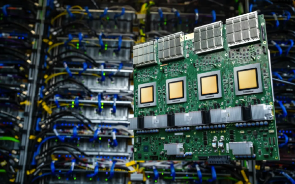
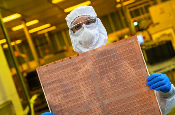
Intel has unveiled a highly modular next-generation advanced packaging concept, underscoring a strategic shift in how performance scaling will be achieved in the coming decade. As transistor scaling on leading-edge nodes becomes increasingly complex and expensive, Intel is doubling down on system-level innovation—combining heterogeneous process nodes, 3D stacking, and high-density chiplet interconnects.
The demonstration integrates 18A and 14A-class nodes, Foveros Direct 3D stacking, and an enhanced EMIB-T bridge with TSVs, presenting a blueprint for future AI and High-Performance Computing (HPC) systems that scale beyond traditional reticle and monolithic die limits.
🏗️ A Modular “System of Chips” Architecture #
Instead of relying on a single massive die, Intel’s design embraces a fully disaggregated architecture, optimizing yield, flexibility, and time-to-market.
Base Layer: Power and Cache Foundation #
The bottom layer uses 18A-PT silicon featuring PowerVia (Backside Power Delivery). Its primary roles include:
- Delivering clean, low-impedance power to upper logic layers
- Hosting large amounts of high-density SRAM, effectively functioning as a giant on-package cache
- Reducing IR drop and improving frequency stability for compute tiles above
This separation of power and logic allows Intel to independently optimize each layer.
Compute Layer: High-Performance Logic Tiles #
The main compute logic is implemented using 14A / 14A-E process technology with RibbonFET 2 transistors. These tiles are vertically stacked on the base layer using Foveros Direct 3D hybrid bonding, enabling:
- Ultra-fine interconnect pitch
- Lower energy per bit transferred
- Significantly reduced inter-tile latency compared to traditional micro-bump stacking
Each compute tile can be tailored independently, allowing heterogeneous cores, accelerators, or domain-specific logic to coexist in the same package.
Horizontal Scaling with EMIB-T #
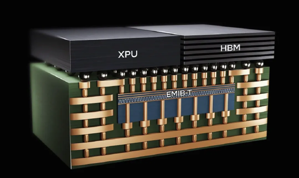
To break past reticle-size constraints, Intel employs EMIB-T, an evolution of its Embedded Multi-die Interconnect Bridge technology that incorporates Through-Silicon Vias (TSVs). This enables:
- Large-scale horizontal expansion
- High-bandwidth, low-latency die-to-die communication
- Better manufacturing yield than full silicon interposers
📦 Extreme Scale and Memory Density #
Intel’s concept design highlights the level of integration it believes will be necessary for next-generation AI training and inference workloads.
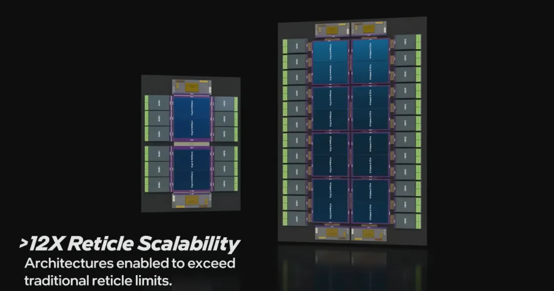
| Component | Maximum Configuration |
|---|---|
| Compute Tiles | Up to 16 |
| HBM Sites | Up to 24 (HBM3E / HBM4 / HBM5 ready) |
| LPDDR5X Controllers | Up to 48 |
| Package Size | Up to 120 × 180 mm |
| Scalability | >12× reticle-scale |
This configuration targets workloads that are both compute-dense and memory-bandwidth-bound, such as large language models and scientific simulation.
⚔️ Direct Competition with TSMC CoWoS-L #
Intel is positioning EMIB-T as a strategic alternative to TSMC’s CoWoS-L packaging technology.
- TSMC CoWoS-L: Relies on a large silicon interposer to connect compute dies and HBM stacks, offering excellent bandwidth but increasing cost and yield risk as interposer size grows.
- Intel EMIB-T: Uses localized silicon bridges embedded in the substrate, avoiding the need for a single massive interposer while still achieving high bandwidth and scalability.
Intel claims that its greater than 12× reticle scalability allows larger system-in-package (SiP) designs with more predictable yields and potentially lower costs at extreme scales.
🧭 Strategic Implications for Intel Foundry Services #
This showcase is not merely a technology demo—it is a foundry-facing statement.
- Node Strategy: Intel has indicated that 18A is primarily tuned for internal products such as Panther Lake and Clearwater Forest, while 14A is being co-developed with external customers to meet HPC and accelerator requirements.
- Packaging as the Entry Ticket: Advanced packaging is no longer optional. For modern AI silicon, it defines performance ceilings, memory bandwidth, and even product viability.
- Future-Proof Memory Support: By decoupling compute logic from memory standards, Intel allows customers to migrate from HBM3E to HBM4 or HBM5 without redesigning the entire compute stack.
🧠 Conclusion #
Intel’s latest packaging showcase makes one point clear: the future of scaling lies above and beyond the transistor. With Foveros Direct 3D, EMIB-T, and a flexible multi-node strategy, Intel is positioning itself as a serious contender not just in process technology, but in full system-level silicon integration.
For AI and HPC customers facing power, bandwidth, and reticle limits, this “system of chips” approach may define the architecture of the next decade.