SSD vs HDD in 2026: Why 30TB SSDs Cost Up to 23x More
The long-running assumption that enterprise storage will inevitably transition from hard disk drives (HDDs) to solid-state drives (SSDs) is facing a major economic reality check.
According to a recent industry report from hybrid-storage vendor VDURA, the price gap between enterprise SSDs and HDDs widened dramatically during the third quarter of 2026. A 30TB enterprise TLC SSD averaged approximately $22,600, compared with just $1,216 for a 30TB enterprise HDD.
That puts the SSD at roughly 18.6 times the cost of an HDD on a capacity-equivalent basis. Earlier in 2026, the gap reportedly reached as high as 23.2x. For comparison, the equivalent price difference was approximately 7x in Q3 2025.
The result is a storage market in which SSDs remain indispensable for latency-sensitive workloads, while HDDs continue to provide an enormous economic advantage for capacity-oriented storage. At the same time, new developments in processing-in-memory (PIM), DRAM, and NAND manufacturing are reshaping the broader memory hierarchy.
💾 Enterprise SSD Economics Have Diverged Sharply From HDDs #
The latest pricing data highlights how dramatically the economics of flash storage have changed.
A 30TB enterprise TLC SSD averaging $22,600 translates to approximately $753 per TB. A comparable 30TB enterprise HDD averaging $1,216 costs only about $40.5 per TB.
The difference is particularly significant for large-scale AI infrastructure, where storage capacity requirements can reach tens or hundreds of petabytes.
Flash pricing is driving the imbalance #
The primary factor behind the widening gap is the sharp increase in flash-memory pricing.
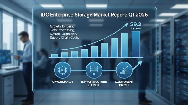
Enterprise SSD prices reportedly increased to approximately 6.5 times their previous level within a year, while HDD prices rose much more gradually. TrendForce data further indicates that enterprise SSD contract prices increased by roughly 80% in a single quarter.
Customers without long-term supply agreements may face even higher prices in spot markets.
This creates a difficult procurement environment for data-center operators: SSDs deliver substantially better latency and I/O performance, but the capacity economics become increasingly difficult to justify when large amounts of data do not require flash-level access performance.
🏗️ Hybrid Storage Can Cut AI Infrastructure TCO #
The economics become even more pronounced at AI-scale storage capacities.
According to the VDURA analysis, building a 25PB AI storage environment entirely with flash could result in a three-year total cost of ownership (TCO) of approximately $51.6 million.
A hybrid architecture combining SSDs and HDDs, while retaining sufficient bandwidth for performance-sensitive workloads, could reduce the three-year TCO to approximately $12.86 million.
That represents a reduction of roughly 75%.
Why HDDs remain relevant #
The performance gap between HDDs and SSDs is undeniable. HDDs cannot approach flash storage in random-access latency, IOPS, or parallel I/O performance.
However, storage architecture is not determined by performance alone.
For cold data, backup repositories, large media datasets, archival workloads, and other capacity-oriented use cases, HDDs continue to offer a compelling cost-per-gigabyte advantage.
Modern enterprise HDDs also employ multi-platter designs to achieve very high capacities while retaining compatibility with established storage infrastructure.
SATA and SAS remain important #
Enterprise HDD deployments continue to rely heavily on established SATA and SAS interfaces.
This matters because storage infrastructure is rarely replaced in isolation. Existing servers, storage arrays, controllers, operating environments, and management software all influence procurement decisions.
As a result, HDDs can remain economically attractive even when SSDs offer dramatically superior raw performance.
🔮 3D DRAM PIM Targets the Memory Wall #
While storage economics remain heavily influenced by NAND and HDD supply, innovation is also occurring closer to the compute layer.
Chinese chip-design company Qianhe Yibang recently announced the successful tape-out and bring-up of what it describes as a four-layer 3D DRAM processing-in-memory (PIM) chip.
The design represents a move from architectural validation toward engineering implementation, with computing and memory resources integrated into a three-dimensional structure.
The “4+1” architecture #
The chip uses a “4+1” stacked configuration consisting of a base logic layer with four vertically stacked DRAM layers above it.
The objective is to increase memory bandwidth and computational density by physically integrating processing resources with memory rather than relying exclusively on conventional planar memory architectures.
This approach directly targets the so-called memory wall: the growing gap between processor computational capability and the ability of conventional memory systems to deliver data quickly enough.
With additional DRAM layers, more resources can be exposed to parallel workloads and high-concurrency data streams.
Engineering complexity increases with stacking #
Higher-density 3D integration also introduces substantial engineering challenges.
Every additional layer increases the difficulty of:
- Inter-layer alignment
- Vertical interconnect reliability
- Manufacturing yield
- Thermal management
- Power delivery
- Package-level reliability
Consequently, successfully moving to four DRAM layers is not simply a matter of adding more memory dies. It requires coordinated advances in architecture, process technology, packaging, thermal engineering, and manufacturing.
Qianhe Yibang describes its implementation as a significant milestone for its 3D-integrated native-computing architecture.
Performance targets across the system #
According to the company, the architecture delivers an order-of-magnitude improvement across several system-level metrics compared with conventional solutions, including data-access bandwidth, memory-access power consumption and latency, data throughput, and processing cost.
Such improvements could be particularly valuable for workloads characterized by massive parallelism and high-concurrency data movement, including cloud gaming and other data-intensive acceleration scenarios.
🔬 Qianhe Yibang Builds Around 3D PIM #
Qianhe Yibang was founded in January 2024 and incubated by NetEase, with a focus on 3D processing-in-memory, 3D-integrated native chip architectures, and acceleration technologies.
Its core team began exploring 3D DRAM PIM architectures and commercialization as early as 2018, when processing-in-memory remained largely an academic research direction.
After multiple tape-outs, experiments, and architectural iterations, the company says it has developed capabilities spanning architecture definition, front-end and back-end design, advanced 3D packaging, and wafer manufacturing.
The company also reports that it has established a complete development and manufacturing chain with domestic supply-chain partners.
Capital and commercialization support #
Qianhe Yibang recently completed a Series B financing round exceeding RMB 2 billion.
Long-term shareholders and partners, including NetEase Youdao and China Mobile Chain Leader Fund, are also expected to provide commercial environments and validation scenarios for the technology.
The combination of financing, application scenarios, and manufacturing capabilities could help accelerate the transition of 3D PIM from specialized research into commercially deployable acceleration hardware.
📈 CXMT Rapidly Expands Its Position in Global DRAM #
The evolution of China’s semiconductor industry is not limited to experimental architectures.
Counterpoint Research’s Q2 2026 Global Memory Tracker reportedly placed ChangXin Memory Technologies (CXMT) fourth in the global DRAM market, with a 7% share.
The company also recorded reported year-over-year revenue growth of 716% during the quarter, making it the fastest-growing DRAM supplier in the period covered by the report.
According to the report, CXMT contributed approximately 11.3% of global DRAM market growth in 2026.
Capacity expansion is a major factor #
CXMT operates three 12-inch DRAM fabs across Hefei and Beijing.
Its combined monthly production capacity is reported at approximately 300,000 wafers, with plans to increase that figure to around 350,000 wafers by the end of 2026.
Capacity utilization has reportedly remained above 90% for an extended period.
For a memory manufacturer, sustained high utilization combined with capacity expansion can provide significant leverage during periods of strong market demand.
The competitive landscape is changing #
The traditional global DRAM market has long been dominated by Samsung, SK Hynix, and Micron.
CXMT’s rapid market-share expansion introduces a significant additional competitor into that structure.
Counterpoint Research Vice President of Research Neil Shah has reportedly characterized the company’s progress as a question of when, rather than whether, it can become one of the world’s leading memory manufacturers.
The combination of China’s large domestic demand, expanding production capacity, and growing memory consumption from AI infrastructure is creating favorable conditions for CXMT’s expansion.
🍎 Apple Is Reportedly Testing CXMT Memory #
The rapid development of CXMT has also attracted attention from major consumer-electronics companies.
Apple is reportedly testing CXMT DRAM for potential use in iPhone and MacBook product lines as the broader memory market faces supply pressure from the AI boom.
The significance extends beyond a single customer.
AI training and inference require enormous quantities of HBM and server memory, increasing demand throughout the broader DRAM ecosystem. As memory manufacturers redirect capacity toward higher-value AI products, conventional PC, smartphone, and data-center memory markets can also experience supply constraints and price increases.
For device manufacturers, additional qualified memory suppliers can therefore become strategically important.
🌐 AI Is Reshaping the Global Memory Market #
The AI infrastructure boom is affecting virtually every level of the memory hierarchy.
At the high end, AI accelerators are driving demand for HBM and high-performance server memory. At the storage layer, AI datasets are increasing the need for high-capacity SSDs and HDDs. Meanwhile, conventional computing products continue to consume large volumes of DRAM and NAND.
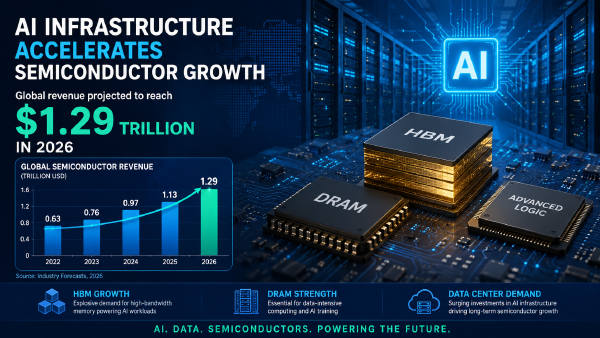
TrendForce forecasts that global DRAM output value could reach approximately $618.7 billion in 2026 and $903.3 billion in 2027.
If these projections materialize, memory will remain one of the most strategically important components of AI infrastructure.
The resulting market dynamics also explain why the economics of SSDs and HDDs have diverged so dramatically. AI increases demand for fast storage, but not every byte of AI-generated data requires flash-level performance.
That distinction makes tiered and hybrid storage architectures increasingly important.
💿 YMTC Advances Its NAND Flash Expansion #
The competitive shift is also visible in NAND flash.
The Shanghai Stock Exchange has reportedly accepted the STAR Market IPO application of Yangtze Memory Technologies Co., Ltd. (YMTC), China’s leading 3D NAND flash manufacturer.
The company plans to raise approximately RMB 33 billion, with the proceeds primarily allocated to production-line expansion, next-generation 3D NAND R&D, and working capital.
Xtacking remains a key technology #
YMTC’s product portfolio is built around its Xtacking architecture and includes high-layer-count 3D NAND products.
The company has achieved mass production of 232-layer NAND and is advancing development toward 294-layer processes.
Its flash products target smartphones, consumer SSDs, enterprise servers, AI data centers, and other storage-intensive applications.
According to TrendForce data cited in the source material, YMTC ranked third globally and first domestically by NAND flash shipment volume and revenue during Q1 2026.
IPO funding could accelerate capacity expansion #
The planned capital raise would provide additional funding for production expansion and next-generation NAND development.
Increasing domestic NAND capacity could help address the rapidly growing storage requirements generated by AI infrastructure while reducing the dependence of Chinese electronics and server manufacturers on overseas memory suppliers.
The company’s ownership structure is also notable. Rather than having a single controlling shareholder, YMTC is held predominantly by multiple state-owned asset platforms, with Hubei Changsheng Development Co., Ltd. reported as its largest shareholder with a direct 26.5442% stake.
🔗 Storage Is Becoming a Multi-Layer Architecture #
The latest developments across SSDs, HDDs, DRAM, PIM, and NAND point toward the same broader conclusion: the future of high-performance computing will not be defined by a single memory or storage technology.
Instead, infrastructure will increasingly depend on a hierarchy of specialized technologies.
SSDs remain essential for latency-sensitive and high-IOPS workloads. HDDs continue to dominate capacity economics for colder and less frequently accessed data. DRAM provides high-speed working memory, while PIM architectures attempt to reduce the data-movement bottleneck by bringing computation closer to memory.
At the manufacturing level, companies such as CXMT and YMTC are expanding domestic DRAM and NAND capabilities, while the broader semiconductor ecosystem continues to invest in higher-density memory and storage technologies.
For AI infrastructure architects, the key question is therefore no longer simply whether SSDs can replace HDDs.
The more important question is which data should live on which storage tier, at what performance level, and at what total cost of ownership.
As flash prices remain elevated and AI workloads continue expanding, that distinction could determine whether a storage architecture is economically viable at petabyte scale.